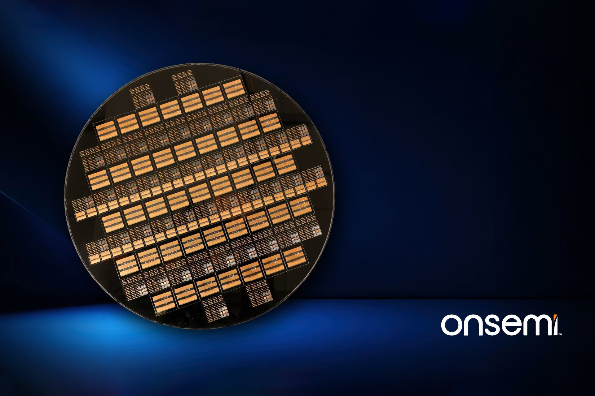
Onsemi has introduced the Embedded Power Platform (EPP), which rethinks power packaging by using the silicon wafer itself as the package, merging electrical, thermal, and mechanical design into a single integrated device. This innovative approach targets key sectors such as AI infrastructure, electric vehicles (EVs), and industrial automation, with Subaru Corporation as one of the early partners ahead of customer sampling slated for 2026.
The EPP incorporates field-effect transistors, drivers, and controllers within a wafer-level architecture that features silicon, silicon carbide (SiC), and gallium nitride (GaN). Onsemi claims that this design offers three to five times higher power density compared to conventional packaging methods and can reduce development cycles to as little as four months.
For EV traction inverters, the platform can decrease power losses by 15% and allows for a single inverter design across various power classes. An EPP-based solid-state circuit breaker has been reported to be approximately 50% smaller and 20% cooler than current designs.
Hassane El-Khoury, President and CEO of Onsemi, emphasized that traditionally semiconductors and their packages have been treated separately. EPP integrates them, enhancing system architecture to keep pace with future innovations in power systems, AI, electrification, and automation.
For more details, you can refer to Onsemi’s official announcement here.